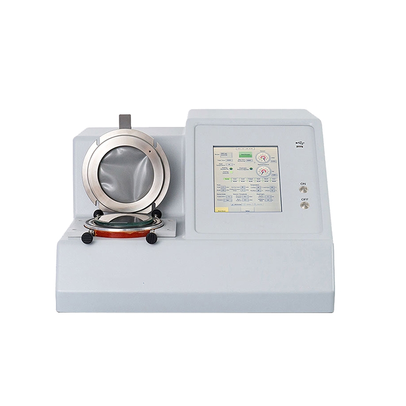
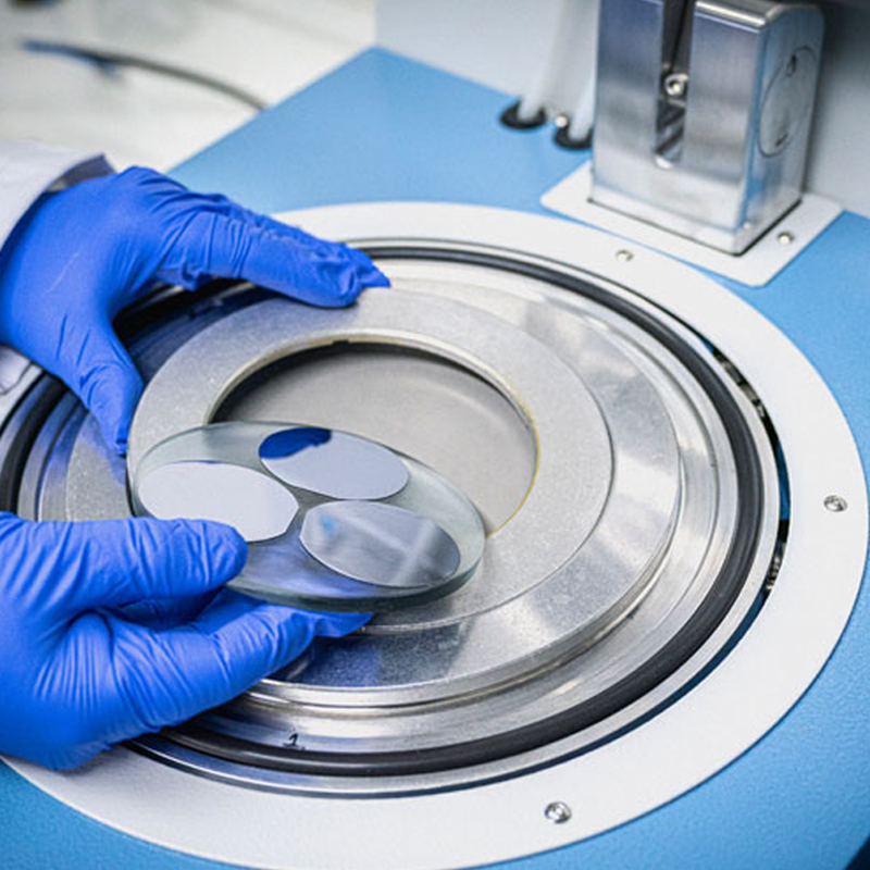
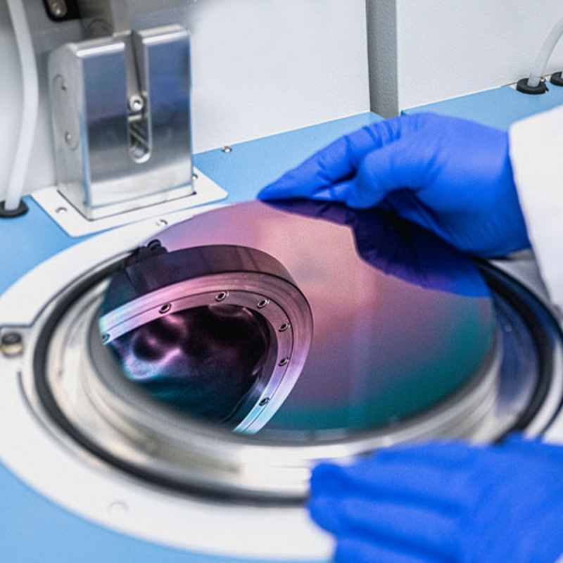
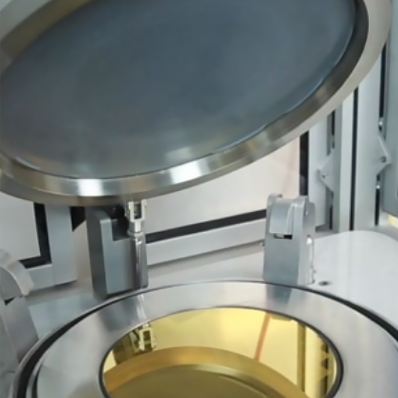
Wafer bonding technology refers to closely bonding two mirrored polished homogeneous or heterogeneous wafers through chemical and physical actions. After wafer bonding, atoms at the interface react to form covalent bonds to form a whole and make the bonding interface reach a specific bonding strength.
Особенности:
Advantages:
Технические характеристики:
| Chamber size | ≤8 inch |
| Temp. range | ≤300℃ |
| Recycling time | 0-60min |
| Voltage | 220V |
Copyright © 2025 ZHENGZHOU HENUO MACHINERY CO., LTD.