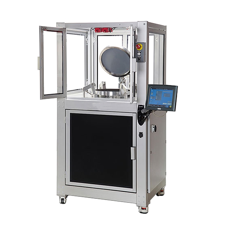
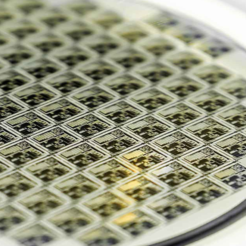
Wafer bonding refers to the technology of connecting wafers and other devices into a new wafer by a physical method. It is a very important technology in modern semiconductor manufacturing technology, widely used in MEMS devices, solar cells, LED wafers and other fields.
Caraterísticas:
Advantages:
Especificações:
| Chamber size | ≤12 inch |
| Temp. range | ≤300℃ |
| Recycling time | 0-60min |
| Voltage | 220V |
Direitos de autor © 2025 ZHENGZHOU HENUO MACHINERY CO., LTD.